Hi Michael.
Three questions:
1) In equations 5 and 6 of TPS63020's datasheet, the "us" parameter is equal to 1/2.4? (It comes from typ. FSW = 2.4Mhz)? Equal to 0,4166666 ?

2) Page 18 shows: A small capacitor C2=10pF (from FB pin to GND), in parallel with R2 needs to be placed when using the Power save mode and the
adjustable version, to provide filtering and improve the considerably the efficiency.
Do I need to place this capacitor if I will use the ajustable version but DON'T want to use Power Save mode?
3) TPS63020's datasheet shows that the maximum voltage that can be applied to ENABLE pin is 7V (absolute maximum rating). Is there any problem if, for example, VIN and VINA = 3V and a 5V signal is applied to ENABLE pin? Maybe this can't be done if there is an ESD protection diode from ENABLE (diode-A) to VIN or VINA (diode-K) internally on the IC. I would like to use a 5V signal to control ENABLE pin...
TPS63020 TESTS...
We have here:
4x TPS63020 ICs
1x TPS63020EVM-487
For all 4 TPS63020 ICs (outside a PCB), we measured electrical conduction between VOUT/L2 pins and between L1/VIN pins, using a multimeter.
For all 4 ICs there was NO conduction from VOUT to L2
For all 4 ICs there was conduction from L1 to VIN
We did some tests with the TPS63020EVM-487. In all tests, ENABLE pin was connected to GND and PSYNC connected do VIN on the EVM.
This EVM comes with the output set to 3.3V.
----------------------------------------------------------------------
(1) An external PSU of +5V was connected to VOUT pin and TPS63020's VIN pin was floating (nothing connected to it).
Result:
VIN to GND: 0V
VFB: 750mV -> This condition would force the TPS63020's switches to OFF state, because VFB is always > 500mV
----------------------------------------------------------------------
(2) After test 1, we connected a Li-Ion BAT with 4.1V to VIN pin of TPS63020, mantaining +5V of the external PSU at VOUT
Result:
VFB: 750mV
There was no conduction from VOUT to VIN. Both TPS63020 and the battery didn't get warm.
----------------------------------------------------------------------
----------------------------------------------------------------------
Then we modified the output voltage of the EVM, that was set to 5V.
----------------------------------------------------------------------
----------------------------------------------------------------------
(3) An external PSU of +4.6V was connected to VOUT pin and TPS63020's VIN pin was floating (nothing connected to it).
Result:
VIN to GND: 0V
VFB: 465mV -> This condition would NOT force the TPS63020's switches to OFF state, because VFB is always < 500mV
----------------------------------------------------------------------
(4) After test 3, we connected a Li-Ion BAT with 2.5V to VIN pin of TPS63020, mantaining +4.6V of the external PSU at VOUT
Result:
VFB: 465mV -> This condition would NOT force the TPS63020's switches to OFF state, because VFB is always < 500mV
There was no conduction from VOUT to VIN. Both TPS63020 and the battery didn't get warm.
Period of this test: more than 10 hours.
----------------------------------------------------------------------
(5) An external PSU of +4.6V was connected to VOUT pin and VBAT = 1.2V, in this condition, the IC is OFF due to VIN underoltage lockout, because VIN < 1.5V
Result:
VFB: 465mV -> This condition would NOT force the TPS63020's switches to OFF state, because VFB is always < 500mV
With some series resistor, we measured little currents flowing from BAT+ to VIN
47K -> 474nA
330K -> 181nA
----------------------------------------------------------------------
(6) Under the same condition of test 4, that is, an external PSU of +4.6V connected to VOUT pin and a Li-Ion BAT with 2.5V connected to VIN.
We used some series resistors from BAT+ to VIN, and measured to following voltages on them, like there was around 5uA flowing from +VBAT to VIN.
VBAT: 2.6V
VFB: 465mV -> This condition would NOT force the TPS63020's switches to OFF state, because VFB is always < 500mV
RSERIE = 4.7K: 24mV -> 24mV / 4.7K = 5.1uA
RSERIE = 10K: 50mV -> 50mV / 10K = 5uA
RSERIE = 15K: 75mV -> 75mV / 15K = 5uA
RSERIE = 22K: 108mV -> 108mV / 22K = 4.91uA
All measures were done with two multimeters
----------------------------------------------------------------------
----------------------------------------------------------------------
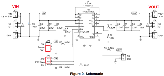
Resistors R5, R4 and R3 were removed from the EVM, because they won't be used in our design.
----------------------------------------------------------------------
----------------------------------------------------------------------
(7) Under the same condition of the previous test, we used some series resistors from BAT+ to VIN, and measured to following voltages on them, like there was some nAs flowing from +VBAT to VIN.
VBAT: 2.6V
VFB: 465mV -> This condition would NOT force the TPS63020's switches to OFF state, because VFB is always < 500mV
RSERIE = 22K: 1.2mV -> 1.2mV / 22K = 54nA
RSERIE = 47K: 1.2mV -> 2.1mV / 47K = 44nA
RSERIE = 100K: 1.2mV -> 3.8mV / 100K = 38nA
RSERIE = 330K: 1.2mV -> 9.8mV / 330K = 29nA
All measures were done with two multimeters
Datasheet shows:

----------------------------------------------------------------------
After all these tests, the TPS63020 of the EVM was working correctly.
Do you have something to say about these tests?
Thanks.