Hi Eric,
I will put my Answers in RED
Charts produced by WEBENCH Designer provide efficiency of ~93.3% and Total Pd of ~1.55W. I don't see any way the charts in the data sheet can produce these values, so which do I believe?
I believe the WEBENCH Efficiency data is calculated at room, temperature so that would make the power dissipation numbers low at elevated temperatures.
Based upon my reading of the curves from the datasheet, I would place the power dissipation at around 2.2 Watts.
1. The example in AN-2020 paragraph 3.1.1 produced board sizes that differed by only 0.030in2, but mine are much farther apart. Which calculation above produces the correct minimum board size?
Example 3.1.1 in An-2020 uses two different calculations based upon how much information is known.
The first equation: Board area (in^2) >= 2.37 * power dissipation makes the following assumptions: 1. Theta JC of the package is close to 7.3C/W, this is the theta JC for a14 pin exposed pad device. Very typical for power. It has other assumptions also such as low thermal impedance from one side of the board to the other (many thermal vias), no airflow etc that are described at the end of the document.
The second equation: Board area (in^2) > 77.5 / (42.5-Theta JC) makes all of the same assumptions except the value of theta JC. Since the module package has a lower theta JC value than 7.3, the second equation will give you a lower board area estimation.
2. Do these calculations assume a 2 or 4-layer board?
These calculations assume a 2 layer board with a copper heat spreader on both layers. Real performance on a two layer board will be slightly worse because heat sinking area will be used for signal routing. The calculations should be close to what would be observed on a 4 layer board where the top inner layer was used exclusivley for ground copper with a large number of thermal vias connected to the DAP to transfer the heat, the ground copper on the outer layers was as unbroken as possible.
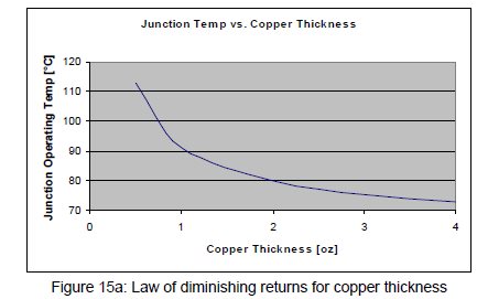
3. I've been unable to find a formula or rule of thumb for using 1oz copper vs 2oz. Is there any reliable guidance on this, beyond AN-2026?
Going from 1 to 2oz's seems to be about a 20-30 percent improvement from what I have seen. Going to more that 2 oz doesn't help as much and the cost is usually prohibitive. Here is a graph I saw in a publication once.
4. Looking at AN-2020 paragraphs 3.2 and 3.2.1, how do I apply the effect of a thermal via array to my calculation of minimum board size? Is it directly additive to Theta JA, producing a proportionately smaller board? The first paragraph on page 19 of the data sheet seems to suggest that it's built into the calculations and thermal vias are simply best practice, with no "reward" (smaller board) for using them.
The simplified equations that we used earlier assume zero thermal impedance from one side of the board to another. They also assume zero thermal impedance to traverse from the hot die to the edge of the board. Those equations are best case. Real results will always be worse. In other words they assume that you have used enough thermal vias such that the top and bottom copper are just two resistances in parallel, and that the copper weight is high enough to spread the heat quickly away from the part.
To add the effect of thermal vias you would also need to add the thermal resistance of the FR-4. All of this is done in the spreadsheet that is linked at the end of AN-2020.
Regards,
Marc